Synopsys has announced an acceleration of development on its yield learning platform designed to speed up ramp up of chips made using Samsung Foundry’s 7LPP (7 nm low power plus) process and newser technologies. The Yield Explorer is a complex yield learning platform that is designed to analyze product layouts, fab data, and product test data in order to find weak spots and enable engineers to improve yields of various chips. Eventually, the Yield Explorer will be enhanced for Samsung’s 5 nm, 4 nm, and 3 nm nodes.
Production of modern chips is an extremely complex process that takes several months to accomplish and involves thousands of steps. Actual yields of chips depend on quality of their designs as well as their power and performance requirements. Therefore, to improve yields of a particular silicon chip, multiple things have to be analyzed to identify systematic yield limiters, and this is exactly what Synopsys’ Yield Explorer does.
The Yield Explorer is a complex set of programs that analyzes data from three sources using advanced machine learning and data visualization techniques. First up, Yield Explorer analyzes product design, including layout and static timings. Secondly, the complex analyzes fab data, including inspection and metrology. Thirdly, the platform considers various product test data, such as binning, system level testing.
| Synopsys' Yield Explorer at a Glance | ||
| Source | Feature | |
| Product design data | Layout, netlist, test diagnosis, static timing analysis | |
| Fab data | Inspection, metrology, wafer acceptance test (WAT) | |
| Product test data | Bin, parametric, system-level test | |
Keeping in mind that silicon design is a property of the designer, whereas information about peculiarities of fab operations and characteristics is confidential, the platform that analyzes yields enables secure collaboration between the foundry and customer.
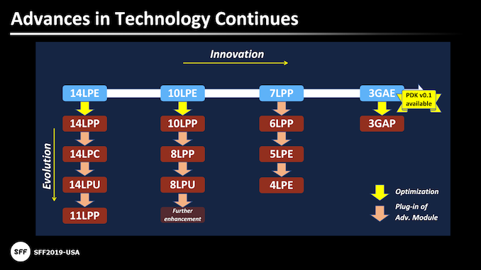
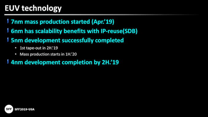
At present, Samsung Foundry and Synopsys offer Yield Explorer for designs produced using 10LPE, 10LPP, 8LPP, 8LPU, and 7LPP fabrication technologies (10 nm, 8 nm, and 7 nm nodes). Compatibility with 7LPP enables the two companies to leverage the platform to 5LPE, 4LPE (and possibly to 6LPP) processes. Furthermore, there is a plan to use Yield Explorer for chips made using 3GAE technology that uses gate all around MBCFET transistors based on silicon nanosheets.
"The secure collaboration model using Yield Explorer has greatly helped us to work efficiently with key customers to achieve target production yields quickly. We look forward to expanding this cooperation with Synopsys as we ramp up production on our 5-nanometer technology node."
- JY Choi, vice president of the Foundry Design Technology Team at Samsung Electronics
Related Reading:
- Samsung Starts Mass Production of Chips Using Its 7nm EUV Process Tech
- Samsung Completes Development of 5nm EUV Process Technology
- Samsung to Invest $115 Billion in Foundry & Chip Businesses by 2030
- Samsung Announces 3nm GAA MBCFET PDK, Version 0.1
Source: Synopsys
from AnandTech https://ift.tt/2Xr9ef7
via IFTTT


0 comments:
Post a Comment