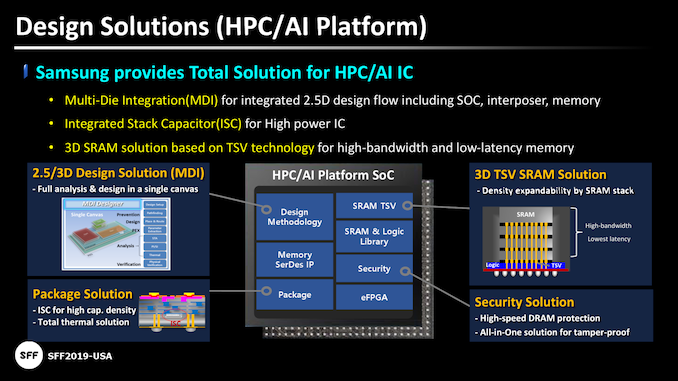
Advanced packaging technologies simplify production and increase performance of highly-complex multi-die SoCs as the semiconductor industry is looking at chiplet approach as an alternative to large dies that take a longer time long to develop and are expensive to make. But designing 2.5D multi-die chips has its own peculiarities, which is why Samsung Foundry and its rivals offer their clients a special 2.5D-IC Multi-Die Integration (MDI) design flow that incorporates analysis and implementation for early-stage system-level pathfinding to help overcome potential issues. This month support for Samsung 2.5D-IC MDI flow was added into Synopsys’ chip development software to simplify development process for engineers.
Samsung Foundry currently offers 2.5D-IC MDI flow for chips produced using its 7LPP (7 nm with several EUV layers) fabrication process and its SUB20LPIN silicon interposer. According to the company, its 2.5D-IC MDI flow helps customers to solve issues like coupling noise between multi-die and package at early stages of design and therefore reduce turnaround time for solving issues (which in the end means lower development costs), overcoming performance problems, and speed up time-to-market. Samsung’s 2.5D-IC MDI flow is now supported by Synopsys’ Fusion Design Platform and Custom Design Platform software packages that are used to develop SoCs.
The programs feature automated silicon interposer creation and routing; routing among microbumps, TSVs, and C4 bumps; power network design; EM/IR analysis of multi-dies and interposer; automated SPICE deck generation for power; and signal integrity analysis of HBM and high-speed interfaces. Functionality of exact software suites is described in the table below.
| Synopsys' Fusion Design Platform and Custom Design Platform supporting Samsung Foundry's 7LPP 2.5D-IC MDI | ||
| Name | Functionality | |
| Fusion Compiler RTL-to-GDSII solution | Fully-automated silicon interposer routing, optimal automated placement and routing among microbumps, TSVs, and C4 bumps. | |
| IC Compiler II place and route | Comprehensive support for interposer creation, inter-die placement and routing, and interposer channel and power routing | |
| RedHawk Analysis Fusion In-Design EM/IR | Seamless In-Design EM/IR analysis of multi-dies and silicon interposer, robust power delivery network design through cleaning missing via, open and short net correlated with ANSYS RedHawk signoff analysis | |
| Custom Compiler design environment | Easy configuration setup based on powerful schematic view and auto SPICE deck generation for power and signal integrity analysis of HBM and high-speed interface (HSI) channels. | |
| HSPICE signal integrity analysis | Linear, transient, and StatEye analysis for PCIe Gen4 | |
| FineSim power and signal integrity analysis | AC and transient analysis for power integrity, crosstalk, jitter, and SSO analysis for HBM | |
By launching its 2.5D-IC MDI flow for 7LPP technology and SUB20LPIN silicon interposer, Samsung Foundry aims to simplify the development process for its customers who adopt multi-die/chiplet approach for their devices aimed at high-performance computing, AI, and other performance-demanding applications. Obviously, quite some time will pass before the first 2.5D devices designed using the 2.5D-IC MDI flow (and Synopsys software) will be brought to fruition, but this is a start.
Here is what Michael Sanie, vice president of marketing and strategy for the Synopsys Design Group, had to say:
“With increasing interest in multi-die integration for accelerating markets such as AI, HPC, and 5G, customers need new solutions because traditional manual design doesn't adequately address the latest power and signal noise challenges. Synopsys' design solutions make a multi-die integration design environment easier and more efficient, and help Samsung Foundry customers deliver faster and higher-performing 2.5D-IC products.”
Related Reading:
- Synopsys to Accelerate Samsung’s 7nm Ramp with Yield Explorer Platform
- Samsung Foundry Updates: 8LPU Added, EUVL on Track for HVM in 2019
- New Tools & IP Accelerate Development of 5nm Arm ‘Hercules’ SoCs
- Samsung Starts Mass Production of Chips Using Its 7nm EUV Process Tech
Source: Synopsys
from AnandTech https://ift.tt/32EMcAi
via IFTTT


0 comments:
Post a Comment