Advanced system-on-chip designs are extremely complex in terms of transistor count and are hard to build using the latest fabrication processes. In a bid to make production of next-generation chips economically feasible, chip fabs need to ensure high yields early in their lifecycle by quickly finding and correcting defects.
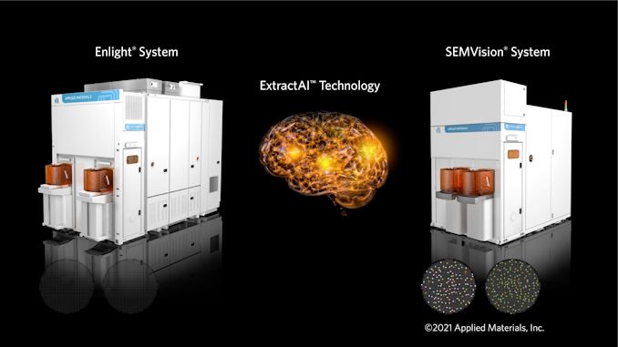
But finding and fixing defects is not easy today, as traditional optical inspection tools don't offer sufficiently detailed image resolution, while high-resolution e-beam and multibeam inspection tools are relatively slow. Looking to bridge the gap on inspection costs and time, Applied Materials has been developing a technology called ExtractAI technology, which uses a combination of the company's latest Enlight optical inspection tool, SEMVision G7 e-beam review system, and deep learning (AI) to qucikly find flaws. And surprisingly, this solution has been in use for about a year now.

from AnandTech https://ift.tt/2QmLNkF
via IFTTT
0 comments:
Post a Comment