Samsung Foundry has made some changes to its plans concerning its 3 nm-class process technologies that use gate-all-around (GAA) transistors, or what Samsung calls its multi-bridge channel field-effect transistors (MBCFETs). Based on new information direct from Samsung, it would appear that its first version of 3nm, 3GAE (3nm gate-all-around early), is coming to high volume manufacturing a year later than expected, but also it seems to have removed this technology from its public roadmap, suggesting it may be for internal use only.
Meanwhile, 3GAE's successor 3GAP (3nm gate-all-around plus) node is still in the roadmap, it is on track for volume manufacturing in 2023.
3GAE on Track for 2022, Maybe Just Not for Everyone
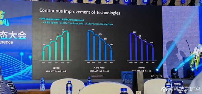
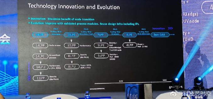
At its recent Foundry Forum 2021 in China, Samsung Foundry presented its updated public technology roadmap which was then republished by bloggers at Baidu and Weibo.
On its FinFET technologies, both 5LPP and 4LPP nodes are new to the roadmap, and set for high-volume manufacturing (HVM) in 2021 and 2022, respectively.
For GAA technology, 3GAE is absent from the roadmap, but 3GAP is there. We reached out to Samsung and a representative confirmed that the 3GAE technology is still on track for ramp in 2022. From the slide, we can see that MBCFET-based 3GAP will enter its HVM phase sometime in 2023.
"As for the 3GAE process, we've been in discussion with customers and expect to mass-produce 3GAE in 2022," the spokesperson said.
The absence of 3GAE process from the public roadmap may be explained by the fact that it will only be available to Samsung's own LSI division, just like some other (E)arly nodes. That being said, previous generation (E)arly nodes are still mentioned in the slides that the company demonstrated.
Samsung originally announced its MBCFET-based 3GAE and 3GAP nodes in May 2019. Back then, the company promised a 35% performance increase, a 50% power consumption reduction, and a 45% area reduction for 3GAE compared to 7LPP. Furthermore, the company announced the availability of v0.1 of its 3nm PDK and at the time said that volume production using 3GAE was set to start in late 2021. With that moving to 2022 based on the latest information, one might interpret this as either a delay or miscalculation based on enabling GAA designs at scale.
However on the plus side, Samsung taped out the first 3 nm test chip several weeks ago. It also announced the availability of Synopsys EDA tools compatible with the new fabrication technologies. The use of fabrication processes that rely on brand-new transistors is always a challenge - in addition to new electronic design automation (EDA) tools, chip developers need all-new IP. We look forward to hearing more disclosures on that front.
A New 4LPP Node on FinFETs
While it looks like general customers are not going to use Samsung's 3 nm nodes until 2023, the newly announced 4LPP is set to meet the requirements of the company's clients in 2022. Since 4LPP relies on familiar FinFETs, it will be much easier for Samsung's customers to use this node when compared to any 3nm GAA nodes early in their lifecycle.
It is noteworthy that Samsung now considers its 5 nm and 4 nm-class technologies as different node branches on its slides. Previously, the foundry considered its 4LPE as an evolution of its 7LPP process. Perhaps this is because 4 nm is set to offer very tangible PPAc (power, performance, area, cost) advantages over 5 nm, or because there are substantial internal changes (e.g., new materials, significantly higher usage of extreme ultraviolet lithography, etc.).
For example, one of Samsung's slides specifically mentions density and performance improvements for 5LPE and 5LPP, but only mentions power and performance improvements for 4LPP. The overlapping technologies will also help to mitigate risks if one of the nodes does not meet certain expectations.
Surprisingly, Samsung Foundry is set to ramp production using its 4LPE and 5LPP technologies at around the same time in 2021, which could enable it to offer different PPAc advantages for different chip designs.
Summary
While Samsung Foundry's GAAFET/MBCFET 3 nm plans appear to have changed and slipped by a year, it is unlikely a big problem for the company as its (E)arly nodes were never widely adopted. To cover that additional year, the company's new 5LPP and 4LPP FinFET-based technologies are set to enable PPA advantages for Samsung Foundry's clients and enable the company to gain more experience with EUV equipment before using it for its 3GAE/3GAP nodes.
from AnandTech https://ift.tt/3k1TQQD
via IFTTT


0 comments:
Post a Comment