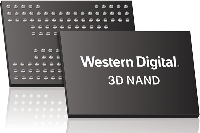
Kioxia and Western Digital formally introduced their 8th Generation BiCS 3D NAND memory with 218 active layers. The new storage device offers a 1Tb capacity in 3D TLC mode and features 3200 MT/s data transfer speed, a combination that will enable SSD makers to build high-performance, high-capacity drives. To enable such an extreme interface speed, the companies adopted an architecture akin to YMTC's Xtacking.
The 218-layer BiCS 3D NAND device jointly developed by Kioxia and Western Digital supports triple-level cell (TLC) and quad-level cell (QLC) configurations to maximize storage density and expand addressable applications. The companies said that the new device embraces their new 'lateral shrink technology to increase bit density by over 50' without elaborating. Considering that the flash memory IC increased the number of active layers by 34%, the claim about a 50% bit density increase indicates that developers also shrank lateral sizes of NAND cells to fit in more of them per layer.
Meanwhile, the 218-layer 3D NAND device features a quad-plane architecture allowing for a higher level of parallelism for programming and read times and increased performance. In addition, the 218-layer 3D TLC device also has a 3200 MT/s (which could provide a 400 MB/s peak read/write speed) input/output interface, which is the highest I/O speed announced so far. High data transfer rates will be handy for high-end client and enterprise SSDs featuring a PCIe 5.0 interface.

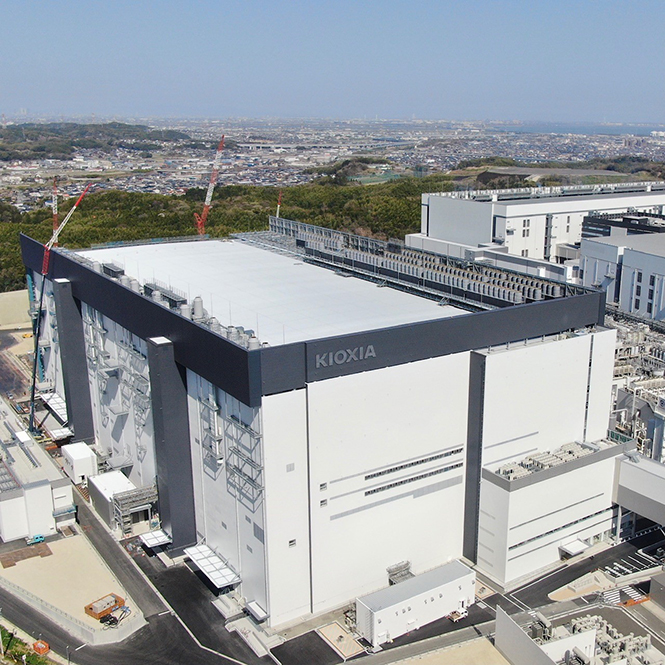
Kioxia and Western Digital Fab 7, Yokkaichi Plant, Japan
The key innovation of the 8th Generation BiCS 3D NAND memory is the all-new CBA (CMOS directly Bonded to Array) architecture that implicates separate production of 3D NAND cell array wafers and I/O CMOS wafers using the most optimal process technologies and then bonding them together to create a final product that offers increased bit density and fast NAND I/O speed. Meanwhile, Kioxia and Western Digital must disclose details about their CBA architecture and whether the I/O CMOS wafers carry other NAND peripheral circuitry, like page buffers, sense amplifiers, and charge pumps.
Producing memory cells and peripheral circuits separately solves several problems as it allows manufacturers to make them using the most efficient process technologies in their sections of cleanrooms. This brings further benefits as the industry adopts methods like string stacking.
Kioxia said it had started sample shipments of 8th Generation BiCS 3D NAND memory devices to select customers. Still, there is no word when the company expects to initiate volume production of its next-generation flash memory. It is not unusual for companies to announce new types of 3D NAND quarters before they enter mass production, so it is reasonable to expect 8th Gen BICS on the market in 2024.
"Through our unique engineering partnership, we have successfully launched the eighth-generation BiCS Flash with the industry's highest 1-bit density," said Masaki Momodomi, Chief Technology Officer at Kioxia Corporation. "I am pleased that Kioxia's sample shipments for limited customers have started. By applying CBA technology and scaling innovations, we've advanced our portfolio of 3D flash memory technologies for use in various data-centric applications, including smartphones, IoT devices, and data centers."
from AnandTech https://ift.tt/GBhQVo0
via IFTTT

0 comments:
Post a Comment