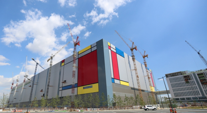
Samsung has begun preparations to build another semiconductor production facility near Pyeongtaek, South Korea. The fab will produce various types of memory as the market demands, and if unofficial information is correct, the new fab may be larger than the adjacent fab that began operations last year.
At present the upcoming fab is called the P2 Project and it will be located adjacent to the existing fab near Pyeongtaek. Samsung has already started to establish infrastructure for the production facility — it ordered the construction of gas pipes for the new production facility in January and is expected to start other works shortly. ETNews reports that Samsung is looking at investing ₩30 trillion ($27.8 billion) in the new P2 Project facility, but does not elaborate whether the number represents total investments, or initial investments. ₩30 trillion is the total amount of money that Samsung has already invested and plans to invest in its existing fab near Pyeongtaek by 2021. Considering the fact that the P2 is in an early stage of planning, it is unlikely that the company has finalized its investments plans.
Officially, a Samsung representative confirmed on Wednesday that the company is considering building a second semiconductor production line near Pyeongtaek. The company anticipates that demand for various memory types will grow in the coming years and therefore has been discussing proactive investments in another production facility. So far Samsung has not decided whether to make DRAM or NAND flash chips in the facility, but considering potential size of the fab, it is possible that Samsung could simply split the facility and do both.
A particularly interesting thing about the P2 Project is the planned timescale. ETNews reports that that the building of the P2 facility “will be completed by the end of the first half of 2019”, which means that construction would need to begin shortly. Once the building is ready, Samsung will have to start equipment move-in. If the company plans to start installation of production tools in mid-2019, then a decision about the equipment (and therefore initial products made at the facility) will have to be made by the end of 2018 at the latest, since tools will need to be procured.
If the new facility is set to produce DRAM, then Samsung will need to buy lithography equipment from companies like ASML or Nikon. If the company decides to produce V-NAND at P2, then it will have to acquire lithography tools as well as a large amount of chemical vapor deposition (CVD) machines and high aspect ratio etch tools from companies like Veeco Instruments, Applied Materials, Adeka and others. Reuters claims that Samsung might start mass production of chips at P2 sometimes in 2020, which corresponds with the ETNews report and indicates that the company has a schedule for its P2 Project.
Assuming that the P2 Project is as large as the company’s existing fab complex near Pyeongtaek, it will take Samsung years to fully ramp up the facility. For reference, the existing fab isn't expected to be fully equipped, expanded and ramped until 2021. Given that the P2 will be used to produce memory chips well into the next decade, it is highly likely that its construction will be ready to accommodate the latest and upcoming production tools, such as EUV step-and-scan systems that will be required to produce DRAM using ultra-thin sub-10nm fabrication technologies.
Related Reading:
- Samsung’s Multi-Billion Fab in Pyeongtaek Starts Production of 64-Layer V-NAND
- SK Hynix to Build a New NAND Fab, Upgrade Existing DRAM Fab

from AnandTech http://ift.tt/2oHOyeP
via IFTTT
0 comments:
Post a Comment