As vehicles are getting ‘smarter’ and gaining autopilot capabilities, it is easy to predict that the demand for higher-performing and more complex automotive SoCs will be growing rapidly in the coming years. To produce those SoCs, specialized manufacturing lines will be needed, which is why the two leading contract chip makers, Samsung and TSMC, are working on new nodes and IP aimed precisely at automobiles.

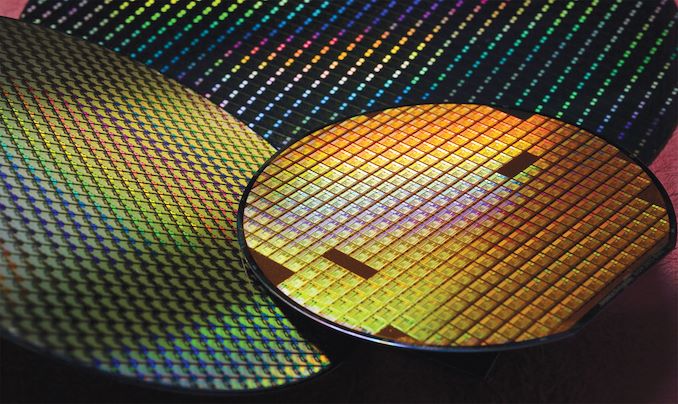
Samsung Foundry this past week said that in the near future it would introduce a version of its 8 nm process for automotive applications. At present, Samsung has two manufacturing processes that are defined as 8 nm: 8LPP and 8LPU, which are evolved from the company’s 10 nm node. It is likely that the automotive-grade 8 nm will be a further evolution of that technology. Right now, the most advanced nodes that Samsung uses to make chips for automobiles are its 28FDS and 14 nm technologies, so an 8 nm node will be a huge step forward.
Samsung did not disclose much about its automotive-grade 8 nm process, but the comapny did note that chips for cars have to comply with AEC-Q100 reliability standards, which mandates support for a -40°C to +105°C ambient operating temperature range, as well as a number of qualification reliability tests such as wear-out tests. Furthermore, to win designs with leading auto makers, these chips have to be made in facilities that have an IATF 16969-certified supply chain quality management system, which in short emphasizes defect prevention and variation reduction. Furthermore, any IP being fabbed, as well as development tools and the final devices themselves have to meet various ISO 26262 (aka ASIL) functional safety requirements, both individually and in context of a particular application.

Meanwhile, over in Taiwan, TSMC’s most advanced automotive-grade process technology today is 16FFC, which is current-generation as far as the automotive market is concerned, as it lags consumer SoC designers by two or three years. Looking towards the near future, TSMC has been developing an automotive-grade version of its N7 (1st Generation 7 nm) technology for quite a while, and expects it to be qualified by 2020. In fact, Synopsys has already developed essential automotive-grade IP for N7 (including DesignWare IP for LPDDR4X, MIPI CSI-2, MIPI D-PHY, and PCIe 4.0 IP), so chip designers are probably already working on new SoCs for vehicles to be made using TSMC’s leading-edge process.

Finally, while GlobalFoundries no longer develops leading-edge process technologies, it still has numerous nodes that can be used by the automotive industry for years to come, including 22FDX and 12LP. For now, these technologies are good enough for advanced SoCs, but it remains to be seen what the company offers to its clients from the auto industry.
Related Reading:
- Samsung Foundry Updates: 8LPU Added, EUVL on Track for HVM in 2019
- Samsung’s 8LPP Process Technology Qualified, Ready for Production
- Samsung’s Intros Exynos Auto V9 SoC: Octa-A76 Chip to Power Audi’s In-Vehicle Infotainment System
- GlobalFoundries and Synopsys Develop Automotive-Grade IP for 22FDX Process Tech
- Arm Unveils Arm Safety Ready Initiative, Cortex-A76AE Processor
- Imagination Launches PowerVR Automotive Initiative, 8XT-A GPU IP
- Bosch and NVIDIA Team Up for Xavier-Based Self-Driving Systems for Mass Market Cars
Sources: Samsung, TSMC, SemiWiki

from AnandTech https://ift.tt/2B9dFxF
via IFTTT
0 comments:
Post a Comment