
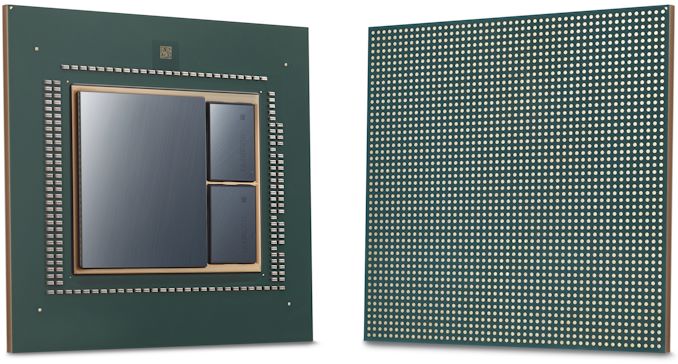
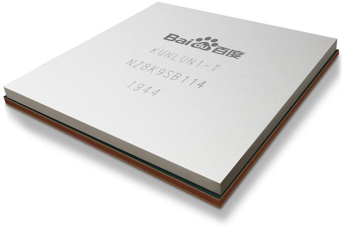
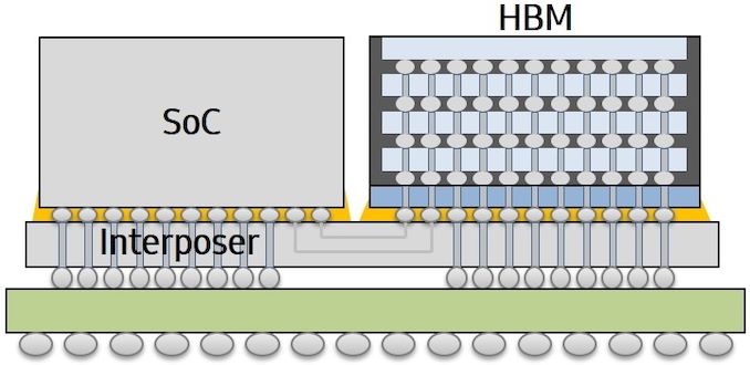
Samsung Foundry and Baidu this week said that the companies were about to start mass production of an AI accelerator chip early in 2020. Baidu’s Kunlun chip is to be made using Samsung’s proven 14 nm process technology, and make use of the company’s Interposer-Cube 2.5D packaging structure.
The Baidu Kunlun AI accelerator is based on the company’s XPU neural processor architecture that uses thousands of small cores that can be used for a wide variety of applications in the cloud and on the edge of networks. The chip provides up to 260 Trillion operations per second (TOPS) at 150 Watts, and features 512 GB/s memory bandwidth using two HBM2 memory packages. It is noteworthy that when the SoC was introduced back in mid-2018, its TDP was described at falling in at 100 Watts, so it seems the final product missed the initial power consumption goals.
According to Baidu, its Kunlun chip is three times faster in the ERNIE (Enhanced Language Representation with Informative Entities) inference application than a traditional GPU or FPGA. In addition, it can be used for autonomous driving (assuming that its 150 W TDP can be mitigated), speech recognition, image processing, and deep learning.
The Kunlun is one of the first AI accelerator that uses I-Cube packaging and is made by Samsung Foundry. The 2.5D packaging uses an interposer and is expected to enable Samsung to build other accelerator chips that require high memory bandwidth, and therefore make use of their HBM2 memory offerings. In addition, the company is developing other advanced packaging solutions, including redistribution layers (RDL), as well as denser HBM packages.
Ryan Lee, vice president of foundry marketing at Samsung Electronics, said the following:
“Baidu Kunlun is an important milestone for Samsung Foundry as we are expanding our business area beyond mobile to datacenter applications by developing and mass-producing AI chips. Samsung will provide comprehensive foundry solutions from design support to cutting-edge manufacturing technologies, such as 5LPE, 4LPE, as well as 2.5D packaging.”
Related Reading:
- Intel's Xeon Cascade Lake vs. NVIDIA Turing: An Analysis in AI
- AI On The Edge: New Flex Logix X1 Inference AI Chip For Fanless Designs
- The AI Race Expands: Qualcomm Reveals “Cloud AI 100” Family of Datacenter AI Inference Accelerators for 2020
- Hot Chips 31 Live Blogs: Xilinx Versal AI Engine
- Cambricon, Makers of Huawei's Kirin NPU IP, Build A Big AI Chip and PCIe Card
Source: Samsung

from AnandTech https://ift.tt/2PzCmvi
via IFTTT
0 comments:
Post a Comment