
Absent from the discrete GPU space for over 20 years, this year Intel is set to see the first fruits from their labors to re-enter that market. The company has been developing their new Xe family of GPUs for a few years now, and the first products are finally set to arrive in the coming months with the Xe-LP-based DG1 discrete GPU, as well as Tiger Lake’s integrated GPU, kicking off the Xe GPU era for Intel.
But those first Xe-LP products are just the tip of a much larger iceberg. Intending to develop a comprehensive top-to-bottom GPU product stack, Intel is also working on GPUs optimized for the high-power discrete market (Xe-HP), as well as the high-performance computing market (Xe-HPC).
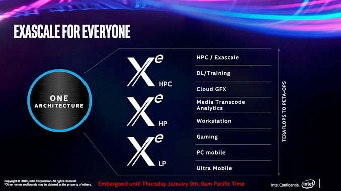
Xe-HPC, in turn, is arguably the most important of the three segments for Intel, as well as being the riskiest. The server-class GPU will be responsible for broadening Intel’s lucrative server business beyond CPUs, along with fending off NVIDIA and other GPU/accelerator rivals, who in the last few years have ridden the deep learning wave to booming profits and market shares that increasingly threaten Intel’s traditional market dominance. The server market is also the riskiest market, due to the high-stakes nature of the hardware: the only thing bigger than the profits are the chips, and thus the costs to enter the market. So under the watchful eye of Raja Koduri, Intel’s GPU guru, the company is gearing up to stage a major assault into the GPU space.
That brings us to the matter of this week’s teaser. One of the benefits of being a (relatively) upstart rival in the GPU business is that Intel doesn’t have any current-generation products that they need to protect; without the risk of Osborning themselves, they’re free to talk about their upcoming products even well before they ship. So, as a bit of a savvy social media ham, Koduri has been posting occasional photos of Ponte Vecchio, the first Xe-HPC GPU, as Intel brings it up in their labs.
BFP - big ‘fabulous’ package😀 pic.twitter.com/e0mwov1Ch1
— Raja Koduri (@Rajaontheedge) June 25, 2020
Today’s teaser from Koduri shows off a tray with three different Ponte Vecchio chips of different sizes. While detailed information about Ponte Vecchio is still limited, Intel has previously commented that Ponte Vecchio would be taking a chiplet route for the GPU, using multiple chiplets to build larger and more powerful designs. Koduri’s latest photo, in turn, looks to be a clear illustration of that, with the larger chip sizes roughly correlating to 1x2 and 2x2 configurations of the smallest chip.
And with presumably multiple chiplets under the hood, the resulting chips are quite sizable. With a helpful 18650 battery in the photo for reference, we can see that the smaller packages are around 65mm wide, while the largest package is easily approaching 110mm on a side. (For refence, an Intel desktop CPU is around 37.5mm x 37.5mm).
Finally, in a separate tweet, Koduri quickly talks about performance: “And..they let me hold peta ops in my palm(almost:)!” Koduri doesn’t go into any detail about the numeric format involved – an important qualifier when talking about compute throughput on GPUs that can process lower-precision formats at higher rates – but we’ll be generous and assume INT8 operations. INT8 has become a fairly popular format for deep learning inference, as the integer format offers great performance for neural nets that don’t need high precision. NVIDIA’s A100 accelerator, for reference, tops out at 0.624 PetaOPs for regular tensor operations, or 1.248 PetaOps for a sparse matrix.
And that is the latest on Ponte Vecchio. Though with the parts likely not shipping until later in 2021 as part of the Aurora supercomputer, it’s likely not going to be the last word from Intel and Koduri on their first family of HPC GPUs.

from AnandTech https://ift.tt/3hZWYZO
via IFTTT
0 comments:
Post a Comment