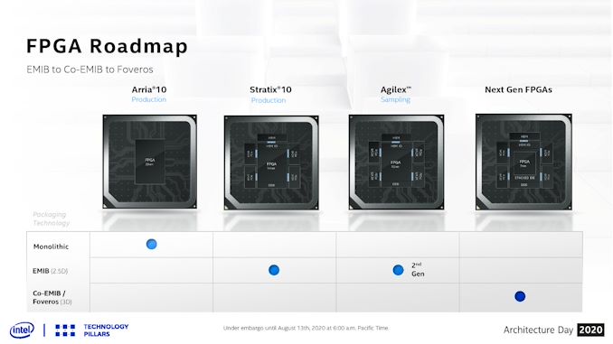
One of the main battlegrounds of future leading-edge semiconductor products will be in the packaging technology: being able to integrate multiple elements of silicon onto the same package with high bandwidth and low power interconnects will be, according to Intel, one way of extending the performance aspects of Moore’s Law into the next decade. Intel has three new parts to its advanced packaging portfolio: EMIB, Foveros, and ODI. At Intel’s Architecture Day 2020, we learned that Intel’s next generation of FPGA products, built on Intel’s own future 7nm manufacturing process, will integrate EMIB from its current generation as well as Foveros 3D stacking.
EMIB, or Embedded Multi-Die Interconnect Bridge, is essentially a bit of silicon embedded into a PCB substrate that allows a silicon die to connect to it in a very dense way. Two bits of silicon can connect to a single EMIB, allowing a fast and low power point-to-point interconnect. We have seen EMIB in use with Kaby Lake-G, the Stratix 10 GX 10M FPGAs, and for upcoming variations of Intel’s Xe graphics portfolio, such as Ponte Vecchio and Xe-HP. Intel has also released a royalty free version of EMIB, called AIB, which has its own generation-on-generation upgrade path for use in the wider industry.
Foveros is Intel’s die-to-die ‘3D’ stacking technology that allows two bits of silicon to connect on top of each other, again in a high-bandwidth and low power implementation. Foveros is currently in use in Intel’s Lakefield mobile processor, and has been announced for future products such as Ponte Vecchio. We now have another one to add to that list: FPGAs.
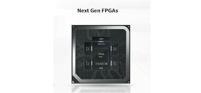
There is no distinct detail about what the next generation FPGAs would have, aside from Intel’s 7nm process and be stacked upon a base die that contains the HBM IO and DDR connections. I assume that the goal here is to have a common base die for a number of FPGA sizes, and then different variants of the 7nm FPGA could be stacked on top based on customer needs, or based on productization perhaps due to yield or cost or such. Technically Intel calls any product with both EMIB and Foveros a ‘Co-EMIB’ product, and this falls under that naming. One of the new elements that the 7nm FPGAs will have access to is a new 224G PAM4 transceiver module, which Intel is currently in the process of tuning and validating.
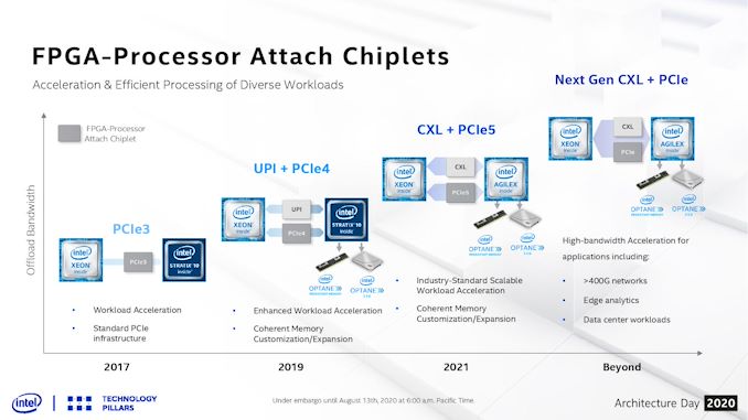
It is unclear exactly when these new 7nm FPGAs will be launched – Intel’s own slide decks show a roadmap where the current 10nm Agilex FPGAs are the main products for 2021/2022, so we are perhaps looking at 2023 or later for these designs. They are far enough out that Intel doesn’t have it on the following roadmap:
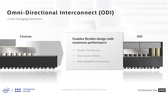
A word on ODI, or Omni-Directional Interconnect. When a chip is built with Foveros, the high-power compute chip often has to be on top for thermal reasons, but the power for that compute chip has to travel through the base chip to reach the compute one. It also means that the top chips are smaller than the ones underneath. ODI solves this issue, by allowing the top chip to ‘hang’ over the edge, in a cantilevered fashion, such that the power connections from the base substrate can rise up through directly to the compute die. If there are enough power connections, then these connections can also be high-bandwidth data connections. This has added benefits in signal integrity, but also added complications in manufacturing and layout.
We expect ODI to be used more in the small-die space first, perhaps in future generations of ‘Lakefield’ type designs, rather than in FPGAs.
Related Reading:
- The Intel Lakefield Deep Dive: Everything To Know About the First x86 Hybrid CPU
- Intel Next-Gen 10-micron Stacking: Going 3D Beyond Foveros
- An Interconnected Interview with Intel’s Ramune Nagisetty: A Future with Foveros
- Intel’s Xe for HPC: Ponte Vecchio with Chiplets, EMIB, and Foveros on 7nm, Coming 2021
- Intel’s EMIB Now Between Two High TDP Die: The New Stratix 10 GX 10M FPGA
- Intel's Interconnected Future: Combining Chiplets, EMIB, and Foveros
from AnandTech https://ift.tt/2YhRoKb
via IFTTT


0 comments:
Post a Comment