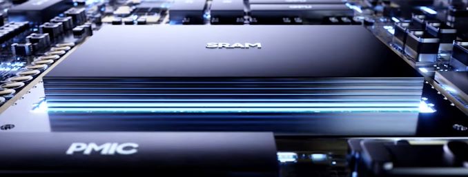
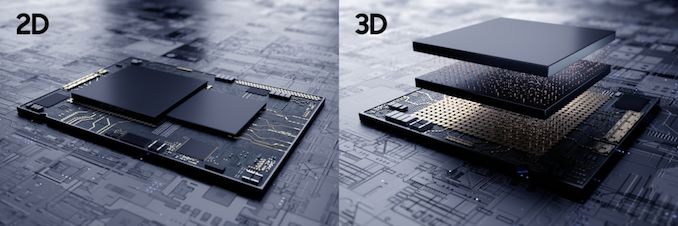
Yesterday, Samsung Electronics had announced a new 3D IC packaging technology called eXtended-Cube, or “X-Cube”, allowing chip-stacking of SRAM dies on top of a base logic die through TSVs.
Current TSV deployments in the industry mostly come in the form of stacking memory dies on top of a memory controller die in high-bandwidth-memory (HBM) modules that are then integrated with more complex packaging technologies, such as silicon interposers, which we see in today’s high-end GPUs and FPGAs, or through other complex packaging such as Intel’s EMIB.
Samsung’s X-Cube is quite different to these existing technologies in that it does away with intermediary interposers or silicon bridges, and directly connects a stacked chip on top of the primary logic die of a design.
Samsung has built a 7nm EUV test chip using this methodology by integrating an SRAM die on top of a logic die. The logic die is designed with TSV pillars which then connect to µ-bumps with only 30µm pitch, allowing the SRAM-die to be directly connected to the main die without intermediary mediums. The company this is the industry’s first design such design with an advanced process node technology.
It’s not the first time that the company has demonstrated TSVs in the base logic die to connect to a stacked die on top of it. Back in 2013, the company had showed custom Exynos chips using Widcon technology, stacking Wide I/O DRAM memory on top of the base logic chip with help of TSVs, offering a higher-performance and lower power solution compared to traditional PoP memory. Unfortunately, this technology never saw the light of day in consumer devices as it likely never was cost-effective enough justify for mass-production.
Stacking more valuable SRAM instead of DRAM on top of the logic chip would likely represent a higher value proposition and return-on-investment to chip designers, as this would allow smaller die footprints for the base logic dies, with larger SRAM cache structures being able to reside on the stacked die. Such a large SRAM die would naturally also allow for significantly more SRAM that would allow for higher performance and lower power usage for a chip.
Samsung’s marketing materials showcase more than a single die of SRAM, which would indicate that X-Cube can be variable in terms of its stack-height. It’s currently unclear if X-Cube will be limited to SRAM dies, or whether it will also extend to future logic-over-logic stacking.
Samsung is providing silicon proven design methodology and flow for its advanced 7nm and 5nm nodes, and states that X-Cube will be utilised for advanced applications such as mobile, AR/VR, wearable and HPC designs. The company is also planning a presentation on X-Cube at Hot Chips this Sunday where it will revealing more details on the technology.
Related Reading:
- AMD Discusses ‘X3D’ Die Stacking and Packaging for Future Products: Hybrid 2.5D and 3D
- Intel's Interconnected Future: Combining Chiplets, EMIB, and Foveros
- The Intel Lakefield Deep Dive: Everything To Know About the First x86 Hybrid CPU
- Samsung Develops 12-Layer 3D TSV DRAM: Up to 24 GB HBM2
from AnandTech https://ift.tt/2PTE9dS
via IFTTT


0 comments:
Post a Comment