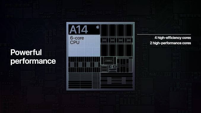
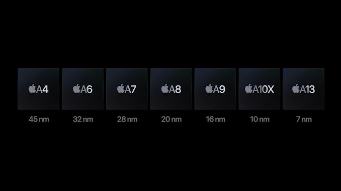
Amongst the new iPad and Watch devices released today, Apple made news in releasing the new A14 SoC chip. Apple’s newest generation silicon design is noteworthy in that is the industry’s first commercial chip to be manufactured on a 5nm process node, marking this the first of a new generation of designs that are expected to significantly push the envelope in the semiconductor space.
Apple’s event disclosures this year were a bit confusing as the company was comparing the new A14 metrics against the A12, given that’s what the previous generation iPad Air had been using until now – we’ll need to add some proper context behind the figures to extrapolate what this means.
On the CPU side of things, Apple is using new generation large performance cores as well as new small power efficient cores, but remains in a 2+4 configuration. Apple here claims a 40% performance boost on the part of the CPUs, although the company doesn’t specify exactly what this metric refers to – is it single-threaded performance? Is it multi-threaded performance? Is it for the large or the small cores?
What we do know though is that it’s in reference to the A12 chipset, and the A13 already had claimed a 20% boost over that generation. Simple arithmetic thus dictates that the A14 would be roughly 16% faster than the A13 if Apple’s performance metric measurements are consistent between generations.
On the GPU side, we also see a similar calculation as Apple claims a 30% performance boost compared to the A12 generation thanks to the new 4-core GPU in the A14. Normalising this against the A13 this would mean only an 8.3% performance boost which is actually quite meagre.
In other areas, Apple is boasting more significant performance jumps such as the new 16-core neural engine which now sports up to 11TOPs inferencing throughput, which is over double the 5TOPs of the A12 and 83% more than the estimated 6TOPs of the A13 neural engine.
Apple does advertise a new image signal processor amongst new features of the SoC, but otherwise the performance metrics (aside from the neural engine) seem rather conservative given the fact that the new chip is boasting 11.8 billion transistors, a 38% generational increase over the A13’s 8.5bn figures.
The one explanation and theory I have is that Apple might have finally pulled back on their excessive peak power draw at the maximum performance states of the CPUs and GPUs, and thus peak performance wouldn’t have seen such a large jump this generation, but favour more sustainable thermal figures.
Apple’s A12 and A13 chips were large performance upgrades both on the side of the CPU and GPU, however one criticism I had made of the company’s designs is that they both increased the power draw beyond what was usually sustainable in a mobile thermal envelope. This meant that while the designs had amazing peak performance figures, the chips were unable to sustain them for prolonged periods beyond 2-3 minutes. Keeping that in mind, the devices throttles to performance levels that were still beyond that of the competition, leaving Apple still being in a leadership position in terms of efficiency.
What speaks against such a theory is that Apple made no mention at all of concrete power or power efficiency figures this generation, which is rather very unusual given they’ve traditionally always made a remark on this aspect of the new designs. We’ll just have to wait and see if this is indicative of the actual products not having improved in this regard, of it’s just an omission and side-effect of the new more streamlined presentation style of the event.
Whatever the performance and efficiency figures are, what Apple can boast about is having the industry’s first ever 5nm silicon design. The new TSMC-fabricated A14 thus represents the cutting-edge of semiconductor technology today, and Apple made sure to mention this during the presentation.
Related Reading:
- The Apple iPhone 11, 11 Pro & 11 Pro Max Review: Performance, Battery, & Camera Elevated
- The Samsung Galaxy S20+, S20 Ultra Exynos & Snapdragon Review: Megalomania Devices
- TSMC Expects 5nm to be 11% of 2020 Wafer Production (sub 16nm)
- ‘Better Yield on 5nm than 7nm’: TSMC Update on Defect Rates for N5
from AnandTech https://ift.tt/3iMGyEl
via IFTTT


0 comments:
Post a Comment