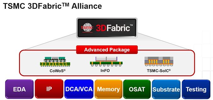
Currently the majority of high-end processors are monolithic, but design methodologies are slowly but surely shifting to multi-chiplet modules as leading-edge fabrication technologies get more expensive to use. In the coming years multi-chiplet system-in-packages (SiPs) are expected to become much more widespread, and advanced 2.5D and 3D chip packaging technologies will gain importance. To accelerate and simplify development of 3D designs, TSMC this week established its 3DFabric Alliance.
While multi-chiplet SiPs promise to simplify development and verification of highly complex designs, they require brand-new development methodologies as 3D packages bring a number of new challenges. This includes new design flows required for 3D integration, new methods of power delivery, new packaging technologies, and new testing techniques. To make the best use of the benefits of TSMC's 2.5D and 3D packaging technologies (InFO, CoWoS, and SoIC), the chip development industry needs the whole ecosystem to work in concert on chiplet packaging – and this is what 3DFabric Alliance is designed to do.
“3D silicon stacking and advanced packaging technologies open the door to a new era of chip-level and system-level innovation, and also require extensive ecosystem collaboration to help designers navigate the best path through the myriad options and approaches available to them,” said Dr. L.C. Lu, TSMC fellow and vice president of design and technology platform.
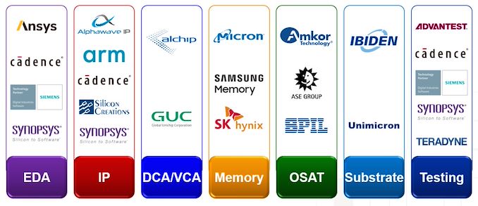
TSMC's 3DFabric Alliance brings together developers of electronic design automation (EDA) tools, intellectual property providers, contract chip designers, memory manufacturers, advanced substrate producers, semiconductor assembly and test companies, and the groups making the equipment used for testing and verification. The alliance currently has 19 members, but over time it is expected to expand as new members join the group.
As the leader of the Alliance, TSMC will set certain ground rules and standards. Meanwhile members of 3DFabric Alliance will co-define and co-develop some of the specifications for TSMC's 3DFabric technologies, will gain early access to TSMC's 3DFabric roadmap and specs to align their plans with the foundry's plans as well as those of other members of the alliance, and will be able to design and optimize solutions that are compatible with the new packaging methods.
Ultimately, TSMC wants to ensure that members of 3DFabric Alliance will offer its clients compatible and interoperable solutions that will enable quick development and verification of multi-chiplet SiPs that use 2.5D and 3D packaging.
For example, to unify the design ecosystem with qualified EDA tools and flows, TSMC has developed its 3Dblox standard. 3Dblox covers various aspects of building multi-chiplet devices featuring 2.5D and 3D packaging methodologies (such as chiplet and interface definitions), including physical implementation, power consumption, heat dissipation, electro-migration IR drop (EMIR), and timing/physical verification.
“Through the collective leadership of TSMC and our ecosystem partners, our 3DFabric Alliance offers customers an easy and flexible way to unlocking the power of 3D IC in their designs, and we can’t wait to see the innovations they can create with our 3DFabric technologies,” added Lu.
Ultimately, TSMC envisions that the alliance will greatly simplify and streamline the process for developing more advanced chips, especially for small and mid-size companies that rely more heavily on outside IP/designs. For example, if a company wants to develop a SiP consisting of logic chiplets stacked together and connected to an HBM3-based memory subsystem, EDA software from Ansys Cadence, Synopsys, and Siemens will allow it to design compatible chiplets, IP providers will sell those blocks the designer does not already have, TSMC will produce silicon, memory producers will offer compatible HBM3 KGSDs (known good stack dies), and then Ase Technology will assemble everything together. Meanwhile companies that do not have their own engineers will be able to order the design of the whole SiP (or individual chiplets) through Alchip or GUC, and then update their product over time if needed without needing to redesign everything, as the SiP will be built in accordance with 3DFabric and 3Dblox standards.
3Dblox is currently supported by four major EDA developers. Eventually it will be supported by all members of the members if the alliance where needed.
While large companies like AMD and Nvidia tend to develop their own IP, interconnection, and packaging technologies, multi-chiplet SiPs promise to make the development of complex, chiplet-style processors accessible to smaller companies. For them, standard third-party IP, fast time-to-market, and proper integration are key to success, so 3DFabric Alliance and what it brings will be vital for them.
Source: TSMC
from AnandTech https://ift.tt/YG1ltiD
via IFTTT


0 comments:
Post a Comment