The head of Samsung's semiconductor unit acknowledged last week that the company's current mass production, leading-edge process technologies are a couple of years behind TSMC's most advanced production nodes. But Samsung is working hard to catch up with its larger rival in five years.
"To be honest, Samsung Electronics' foundry technology lags behind TSMC," said Dr. Kye Hyun Kyung, the head of the Samsung Electronics Device Solutions Division, overseeing global operations of the Memory, System LSI and Foundry business units," at a lecture at the Korea Advanced Institute of Science & Technology (KAIST), reports Hankyung. "We can outperform TSMC within five years."
Samsung has been investing tens of billions of dollars in its foundry division in the recent years in a bid to catch up with TSMC and Intel, both in terms of production capacity for LSI chips as well as process technology advantages. The company has significantly closed the gap with its rivals, but it is still not quite on par with TSMC's fabrication technologies when it comes to performance, power, area (transistor density), and cost metrics.
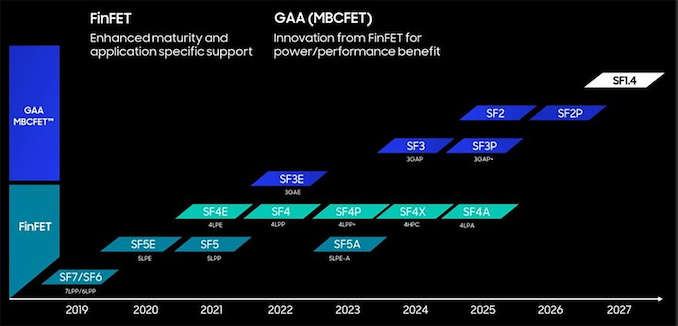
While Samsung Foundry is the first contract maker of chips to adopt gate-all-around (GAA) transistors with its SF3E (3GAE, 3 nm, gate-all-around early) node, and the company's customers are enthusiastic about the technology itself and the novel transistor architecture, this process is not used for Samsung's own leading-edge system-on-chips for smartphones.
"Customers' response to Samsung Electronics' 3nm GAA process is good," said Dr. Kye Hyun Kyung.
Meanwhile, Samsung's latest Galaxy S23-series uses Qualcomm's Snapdragon 8 Gen 2 SoC is made by TSMC on its N4 fabrication process.
Samsung Foundry's most advanced technology that can be used to make highly-complex SoCs for smartphones or other demanding applications is SF4 (4LPP, 4 nm, low-power plus), which, as the company admits, is significantly behind TSMC's N3 (N3B) node, is rumored to be used for mass production of Apple's highly-complex SoCs at this time.
The company may somewhat close the gap with TSMC's N3 and N4P with its SF4P (4LPP+) that will be available for customers later this year, according to a clarification published by @Tech_Reve.
Samsung Foundry will have a better chance to catch up with TSMC when its SF3 (3GAP) fabrication node enters high volume production in 2024, though by the time TSMC will also be offering its more advanced N3P manufacturing technology. Around the same time Samsung also plans to offer SF4X (4HPC), a 4 nm-class fabrication technology that will (as the name suggests) address high-performance CPUs and GPUs.
Samsung reportedly believes that transition to GAA transistors in the 2022 ~ 2023 timeframe makes a great sense since it will have time to fix teething problems of the new architecture ahead of its rivals, most notably Intel and TSMC. As a result, when they start fabbing chips on their 2 nm-class technologies (20A, N2) in 2024 – 2025 and possibly encounter the same issues that Samsung is solving today, its SF2 node will be able to offer a better combination of power, performance, transistor density, costs, and yields.
Source: Hankyung.com (via @Tech_Reve)
from AnandTech https://ift.tt/uH1Le2c
via IFTTT


0 comments:
Post a Comment