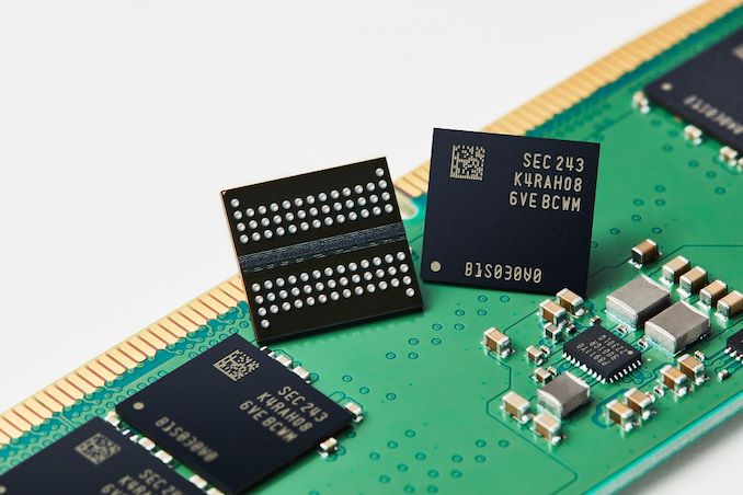
Samsung on Thursday said it had started high volume production DRAM chips on its latest 12nm fabrication process. The new manufacturing node has allowed Samsung to reduce the power consumption of its DRAM devices, as well as decrease their costs significantly compared to its previous-generation node.
According to Samsung's announcement, the company's 12nm fabrication process is being used to produce 16Gbit DDR5 memory chips. And while the company is already producing DDR5 chips with that capacity (e.g. K4RAH086VB-BCQK), the switch to the newer and smaller 12nm process has paid off both in terms of power consumption and die size. As compared to DDR5 dies made on the company's previous-generation node (14nm), the new 12nm dies offer up to 23% lower power consumption, and Samsung is able to produce 20% more dies per wafer (i.e., the DDR5 dies are tangibly smaller).
Samsung says that the key innovation of its 12nm DRAM fabrication process is usage of new high-k material for DRAM cell capacitors that enabled it to increase cell's capacitance to boost performance, but without increasing their dimensions and die sizes. Higher DRAM cell capacitance means a DRAM cell can store more data and reduce power-draining refresh cycles, hence increasing performance. However, larger capacitors typically result in increased cell and die size, which makes the resulting dies more expensive.
DRAM makers have been addressing this by using high-k materials for years, but finding these materials is getting trickier with each new node as memory makers also have to take into account yields and production infrastructure they have. Apparently, Samsung has succeeded in doing so with its 12nm node, though it does not make any disclosures on the matter. That Samsung has succeeded in reducing their die size by a meaningful amount at all is quite remarkable, as analog components like capacitors were some of the first parts of chips to stop scaling down further with finer process nodes.
In addition to introducing a new high-k material, Samsung also reduced operating voltage and noise for its 12nm DDR5 ICs to offer a better balance of performance and power consumption compared to predecessors.
One of the aspects about Samsung's 12nm DRAM technology is that it looks to be the company's 3rd Generation production node for memory that uses extreme ultraviolet lithography. The first D1x node was purely designed as a proof of concept and its successor D1a, which has been in use since 2021, used EUV for five layers. Meanwhile, it is unclear to what degree Samsung's 12nm node is using EUV tools.
"Using differentiated process technology, Samsung’s industry-leading 12nm-class DDR5 DRAM delivers outstanding performance and power efficiency," said Jooyoung Lee, Executive Vice President of DRAM Product & Technology at Samsung Electronics.
Meanwhile, Samsung is also eyeing faster memory speeds with their new 12nm DDR5 dies. According to the company, these dies can run as fast as DDR5-7200 (i.e. 7.2Gbps/pin), which is well ahead of what the official JEDEC specification currently allows for. The voltage required isn't being stated, but if nothing else, it offers some promise for future XMP/EXPO memory kits.
from AnandTech https://ift.tt/HsT0wuX
via IFTTT

0 comments:
Post a Comment