Samsung today announced that it has started mass production of its first commercial embedded Magnetic Random Access Memory (eMRAM). Made using its 28FDS (28nm FD-SOI) process technology, the eMRAM module promises to offer higher performance and endurance when compared to eFlash. Furthermore it can be integrated into existing chips, according to the manufacturer.
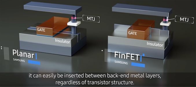
Magneto resistive RAM uses a resistance-based method that determines what data is stored in a cell, which in turn is based on reading the orientation of two ferromagnetic films separated by a thin barrier. Samsung calls this process Magnetic Tunnel Junction, or MTJ.
MRAM is one of the highest-performing and most durable non-volatile memory technologies currently exists. Because its eMRAM does not require an erase cycle before writing data, it is 1,000 times faster than eFlash, Samsung says. It also uses lower voltages when compared to eFlash, and therefore consumes around 1/400th the energy during writing process, according to the maker.
On the flip side, however, MRAM’s density and capacity both fall far short of 3D XPoint, DRAM, and NAND flash, which greatly reduces its addressable markets. Samsung is not formally disclosing the capacity of its new eMRAM module; the company is only saying that it yet has to tape out a 1 Gb eMRAM chip in 2019, which strongly suggests that the current offering has a lower capacity.
Made using Samsung’s 28FDS process technology, Samsung's eMRAM module can be integrated in the back-end of a chip's manufacturing process by adding three additional masks. As a result, the module does not necessarily depend on what front-end manufacturing technology is used, allowing it to be inserted into chips produced using bulk, FinFET, or FD-SOI fabrication processes.
Given its limited capacity, Samsung says that the module is primarilly aimed for use in microcontrollers, chips for IoT, and AI (neural network, machine learning, etc.) applications.
Meanwhile, Samsung says that it will keep expanding its embedded non-volatile memory offerings going forward. Among the upcoming options is its 1 Gb eMRAM test chip, whose tape-out is scheduled for later this year. Farther down the line still, Samsung is also planning to make eMRAM using its 18FDS process, as well as more advanced FinFET-based nodes.
Related Reading:
- IBM And Everspin Announce 19TB NVMe SSD With MRAM Write Cache
- Seagate Demos New SSD Features And Prototypes At FMS
- Everspin Announces New MRAM Products And Partnerships
- MRAM Developer Day, GlobalFoundries Keynote Live Blog
Source: Samsung
from AnandTech https://ift.tt/2XKfs6H
via IFTTT


0 comments:
Post a Comment